The Atom Chip
Trinker, M., Groth, S., Haslinger, S., Manz, S., Betz, T., Schneider, S., Bar-Joseph, I., Schumm, T. & Schmiedmayer, J.
Multilayer atom chips for versatile atom micromanipulation
Applied Physics Letters, 2008, Vol. 92(25), pp. 254102
The central part of the experimental setup is the atom chip and the surrounding assembly. With the exception of small homogeneous external bias fields, all trapping fields in our experiments are provided by the chip itself or by the copper structures mounted directly underneath. This necessitates independent electrical access to as many as 45 different contact points inside the vacuum chamber; eight of these connections need high current tolerances of 50–100A (the others only up to 2A). The resulting complex construction of various UHV-compatible ceramics and metal holders, copper connectors, special alloy pins, isolating Kapton foils etc. consists of several hundred custom made pieces.
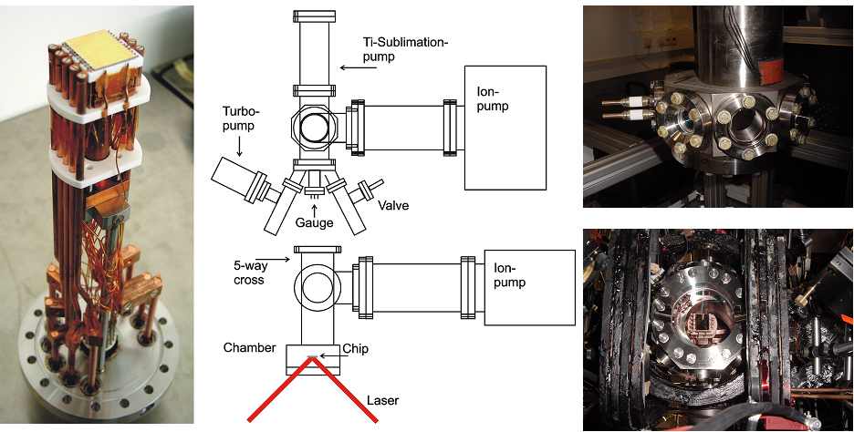 (left) Atom chip assembly: The U-wire structure for the MOT and an additional structure containing Z-shaped wires in several sizes are connected to high-current vacuum feedthroughs. The atom chip is mounted directly on top of these wire structures. (center) Schematic drawing of the vacuum chamber. The actual science chamber consists only of a small octogonal steel body (small rectangle at the bottom of the picture) containing the atom chip. The rest of the chamber serves mainly vacuum diagnostics and allows fast and efficient pumping. (right) Photograph of a clear view of the chamber before (top, side view) and after (bottom, bottom view) optics and coils were mounted.
  Layout of a multilayer atom chip. Left: General view of the chip, size 25 x 30 mm. Contact pads are arranged around the edge of the chip. Wires for trapping of atoms run from top to bottom (blue) on the upmost layer of the chip. Where these wires cross structures on the ground plane, polyimide pads provide insulation of the layers. For longitudinal confinement of the atoms, the chip contains four additional 500 µm wide wires (dark blue) on the ground plane. Upper right: Central part of the chip (600 x 600 µm^2), created by e-beam lithography. Lower right: Detail of this central section (100 x 100 µm^2), similar to the region shown in the SEM micrograph shown below. Three 10 µm wide wires (blue) cross submicron structures (light blue, smallest features: 300 nm wide gaps) separated by polyimide pads.
SEM micrograph of the central part of a multilayer chip. 10 µm wide wires with a height of 1.4 µm cross structures created by e-beam lithography. The smallest features are 300 nm gaps between 700 nm wide and 140 nm high wires. Electrical insulation of the two layers is provided by 500 nm thick polyimide pads, visible as partially transparent layer.