Magnetic Field Sensor
Wildermuth, S., Hofferberth, S., Lesanovsky, I., Haller, E., Andersson, L., Groth, S., Bar-Joseph, I., Krüger, P. & Schmiedmayer, J.
Microscopic magnetic-field imaging
Nature, 2005, Vol. 435, pp. 440
Trapped cold atoms are ideal magnetic sensors as they are very sensitive to changes in magnetic-field landscapes, even in the presence of large homogeneous offset fields. Density modulations in trapped thermal atomic clouds have already been used as a measure of magnetic field variation caused by irregular current flow in nearby conductors. We have produced a versatile, high-resolution sensor based on BECs. Its sensitivity is not limited by the temperature T of the cloud, but is rather determined by the chemical potential µ of the condensate, which can be orders of magnitude lower than kBT.
A BEC is trapped at the measurement site so that its density profile can be directly imaged. The spatially varying density is a measure of the potential energy and hence of the local magnetic-field variation. To probe spatial magnetic-field variations, we start by confining a one-dimensional BEC (in which µ is smaller than an energy quantum of transverse excitation) in an elongated magnetic microtrap with strong transverse and weak longitudinal confinement, created by small conductors mounted on the surface of an atom chip.
As a demonstration, we measured the magnetic-field variations above the 100-µm wide current-carrying wire used to create the trap itself. Scanning the position of the BEC enabled us to reconstruct a full two-dimensional magnetic-field profile near the wire with unprecedented accuracy (sensitivity of 4 nanotesla) at the measurement resolution (3 µm). From this map, we reconstructed the local current flow in the wire and found extremely small angular deviations from a straight current path.
We also investigated an independent field landscape by placing a BEC close (5 µm) to a test wire structure. As long as this structure is grounded and carries no current, the atomic density profile is homogeneous within the detection sensitivity. This corresponds to an upper bound in potential roughness of less than 10-14 eV, corresponding to a temperature of 200 picokelvin (field sensitivity of 300 picotesla). As soon as a small current (about 5 mA) is passed through the wire, a characteristic field profile is imaged.
The technique is applicable not only to magnetic fields, but can also be used to detect variations in electrostatic fields, as can be shownby charging the probed structure electrically. This measurement is more sensitive than the one discussed above because the trapping parameters can be adjusted independently from the measured potential landscape by using a separate wire for holding the BEC.
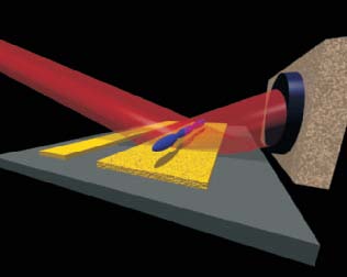 Experimental set-up. A Bose-Einstein condensate is created and trapped by a currentcarrying wire mounted on a silicon surface (atom chip) and is positioned above the sample to be probed.
 The optimal potential sensitivity of a BEC used as a field sensor, ΔB = γΔN/z0 3, is achieved if the trapping parameters are adjusted so that the cloud’s transverse size matches the desired spatial resolution z0. Here ΔN is the minimal atom-number variation resolved by the imaging system, and γ contains all the atomic-physics parameters of the specific atom (γ=8.63·10-29 tesla cubic metres for the 87Rb used in our experiment). Currently available CCD (charge-coupled device) cameras allow atom-shot noise-limited detection with a ΔN value of better than 10 atoms per pixel in absorption imaging, so that a sensitivity, ΔB, of 1 nanotesla is possible even at a high spatial resolution of 1 µm (or 1 picotesla at 10 µm). By changing to a different atom with higher mass and/or by reducing the interatomic interaction, a significant increase in sensitivity can be achieved.
A comparison of different magnetic-field measurement techniques shows that BECs as magnetic sensors could reach unprecedented sensitivity over a large range of spatial resolution. The sample measurements we present here reach higher sensitivities than those obtained with established techniques operating at the same spatial resolution.
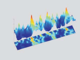 Two-dimensional scan of the magnetic landscape (field component along the wire direction) above a 100-µm-wide an 3.1-µm-tall gold wire. This profile has been reconstructed from 28 equally spaced onedimensional atomic-density traces measured 10 µm above the current-carrying wire at a homogeneous offset field of 2millitesla, so that relative field variations of only 4 p.p.m. stemming from slightly irregular current flow could be measured at a spatial resolution of 3 µm.
 Magnetic field reconstruction:
The local density of the trapped BEC is imaged in situ by high resolution (3 µm) absorption imaging. This experimentally determined density profile n1d(z) is a map of the spatial profile of the field component BIP. The highest sensitivity for detecting variations in BIP is reached by minimizing the chemical potential µ. In our elongated traps, µ is smaller than the energy level spacing in the transverse (tight confinement) direction (µ < hωtr), but much larger than the energy level spacing in the longitudinal (weak confinement) direction (µ >> hωl). In this so called one-dimensional Thomas- Fermi (1dTF) regime, the external potential energy and hence the longitudinal field component profile can be computed. The figure below shows a typical n1d(z) profile and illustrates how a one-dimensional BIP(z) trace is derived from it. The field sensitivity of a single shot measurement is given by the detection noise of n1d which in principle is limited by atom shot noise. In our measurements shown in the figure below we find a single shot sensitivity for a field measurement of ΔB = 4 nT which corresponds to a potential energy change of ΔU ~ 10-13 eV. This sensitivity is reached at an offset field of 10 G, thus the relative detected inhomogeneities are ΔB/B = 4·10-6 (inset in the figure below). The trap used for these measurements had an oscillation frequency of ωtr=2π·3kHz, corresponding to a transverse extension of the condensate (single particle ground state size) of ~ 200 nm. In a second series of experiments we have measured the field profile near an independent wire structure. Here, we have employed a more relaxed trap (ωtr=2π·200Hz), leading to an order of magnitude higher sensitivity of ~ 300 pT in magnetic field units.
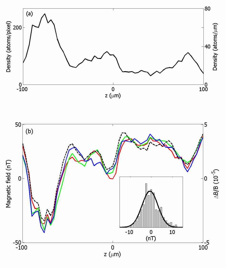 Magnetic field reconstruction from a density profile of a BEC. (a) From imaging the density variations in a BEC onto a CCD-camera using resonant laser light a typical onedimensional density profile n1d(z) can be obtained. (b) From this the longitudinal magnetic potential can be calculated. A section of a 1dTF BEC gives the magnetic field change over the range of 200µm within one experimental shot. The three solid curves (red, green and blue) have been taken at the same experimental parameters (10G homogeneous offset field) and show the good reproducibility of our field measurement. The black (dashed) curve has been reconstructed from a density profile taken with three times higher current in the wire (and three times larger homogeneous offset field). The potential trace has been plotted according to the calculated ΔB/B (right axis), which corresponds to a scaling with the wire current (offset field). The agreement between the ΔB/B measurements using two largely different currents confirms that the potential variations indeed originate from magnetic fields caused by irregular current flow through the wire. The inset shows the shot to shot pixelwise variations of the reconstructed magnetic field for several repetitions of the experiment yielding a single pixel, single shot field sensitivity of 4nT. The spatial resolution of our diffraction limited imaging system is 3µm. The transverse trapping frequency of the trap used in these measurements was ωtr = 2π·3kHz.
 Mapping magnetic fields and current flow reconstruction:
The image of the longitudinal magnetic field component depicted in the figure below of the main text is obtained by scanning the position of the BEC over the entire width of the 100 µm wide 3.1 µm thick trapping wire in a plane parallel to the wire (chip) surface at a distance of 10 µm. The magnetic trap and the cooling are configured in such a way that the condensates form in the 1dTF regime and extend over a large longitudinal stretch of the wire (~1 mm) while they can be transversely positioned with a precision better than 1 µm. This is achieved by using additional images taken from a direction close to perpendicular to the atom chip surface to calibrate the positions relative to defined markers (wire edges). In order to derive a full two-dimensional magnetic image, we have formed condensates at 28 equally spaced transverse positions above the wire covering a width that slightly exceeds that of the wire. The fact that the nominal wire field is exactly compensated at the trap position makes our technique applicable for arbitrary wire currents. From this two-dimensional magnetic landscape the transverse component of the twodimensional current density in the trapping wire can be reconstructed. The current reconstruction is only reliable at a resolution level comparable to the distance from the wire where the magnetic field is scanned (10 µm). More details can be revealed and the full resolution of the sensor can be exploited when the atom-surface distance is further reduced. It has been shown that a surface approach of single microns is possible. Constraints are the limited trap depth in the presence of attractive surface potentials and the finite trap lifetime. Trap lifetimes have to be sufficiently long for the condensate to reach thermodynamic equilibrium. This is typically not problematic as lifetimes on the order of seconds can be achieved down to single micron distance from insulators or thin conducting layers that are prone to be probed by BEC sensors.
 The maximal current density jField sensitivity versus spatial resolution for state-of-the-art magnetic microscopes. MFM and hall probes, operate at a high spatial resolution whereas SQUIDs and thermal atom magnetometers offer high field sensitivity. Typical operation temperatures of the field sensor are indicated. The demonstrated BEC sensor allows mapping of magnetic fields in an intermediate parameter range (4nT at 3µm). Positioning the BEC over an independent sample and thus lowering the transverse confinement has allowed to measure magnetic fields with one order of magnitude higher sensitivity. On the right axis sensitivity is given in units of eV since a BEC can be used to also map other local potentials (for example electric fields) with high spatial resolution. The dark grey shaded region indicates the sensitivity-resolution range currently accessible only to the BEC sensor. The solid (dashed) line displays the estimated sensitivity for a single shot measurement if the trapping potential is optimally adjusted to the desired resolution. Maximal spatial resolution is limited to 500nm by the imaging technique using blue laser light. Field sensitivity is estimated to be 1pT at a spatial resolution of 10µm (corresponding to 1Hz oscillation frequency). For higher field sensitivity (dashed line) and thus low oscillation frequencies, long trap lifetimes are required to reach equilibrium. To estimate the potential sensitivity of the BEC sensor (solid line) a shot noise limited atom detection of 100 atoms (ΔN=10) has been assumed.
Write a comment