Fabrication
For each of the different experiments devices such as Atom Chips and superconducting microwave resonators (QuIC) are fabricated in the clean room facilities of the ZMNS.
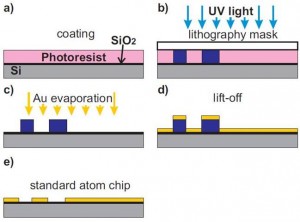
For the production of the Atom Chips a lift-off process adapted from semiconductor nanofabrication techniques is employed. The substrate for the micro structured devices is a single crystal Silicon wafer.
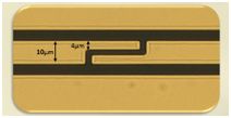
A layer of gold acts as an optical mirror and carries the high currents needed for trapping the atoms. The thermally evaporated gold layer is structured using photosensitive resist, which is then removed in a lift-off process.
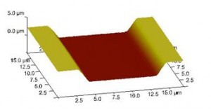
Layer thicknesses up to 3.5 µm have been realized to allow for high currents. The surface roughness of the gold layer is then measured by atomic force microscopy (AFM).
Additionally, SU8 structures can be realized on the gold surface to hold fiber based fluorescence detectors, which can be seen on the Atom Chip used in the Micro Optics experiment.
 For the coplanar waveguide resonators a thin film of Niobium is sputtered on a sapphire substrate. The Niobium is then structured using photosensitive resist and a laser writer. The laser writer operates at a wavelength of 407 nm enabling a resolution down to 0.6 µm. It allows for rapid prototyping as new chip layouts can be written directly into the photoresist without the need of a mask. The micro structured photoresist then acts as a mask for the subsequent etching process in a reactive ion etching (RIE) chamber.


